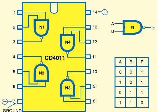
CD4011 is the most commonly used complementary metal oxide Semiconductor (CMOS) chip.The IC comprises of 14 pins with four independent NAND gates (N1,N2,N3,N3) in a single chip. Each NAND gate has two inputs and one output.The working of cd4011 IC requires 5V to 16V to operate. Each output can deliver output current of about 10mA at 12V but this range can reduce as the power supply voltage reduces.The positive terminal of the battery was connected to the pin 14 and negative terminal of the battery was connected to the pin7 .The output pins of the IC are 3,4,10,11 and input pins are 1,2,5,6,9,8,12,13.Now let us see how this Integrated circuit works and how can we use it for our operations.
WORKING OF CD4011:
The operation of this IC was very simple to understand if we understand the operations of NAND gates.As you can see in the above diagram the NAND gates N1….N4 was wired independently and there is no dependency on other gates.So the operation of the IC was completely based on the NAND gate property.We can see the state of the output pins with the assigned inputs in the truth table given above.There we can see that the NAND gate gives a high output to all the input states except the input states 1,1.The combined action of the these four gates form the working of this IC CD4011.
You may have a question that why cant we use single NAND gates instead of this IC since it has the same function as NAND gate.Let me tell you why, usage of large range of the NAND gates occupies more space and also it withdraws more power arising problems in power management to a circuit.This IC was used since it withdraws only small power and also reduces the complexity of the circuit.Still not clear?? let me narrate with an simple example.
EXAMPLE:
Consider these two gates as gates in the IC CD4011 and we are only using two NAND gates in it.This circuit was wired as a door open indicator which indicates the opening of door using the bulb which was connected to the output pins of the gates.Here in this circuit the input pins of the are connected to the supply voltage directly as shown in the diagram.When the door was closed push button switch, it apply logic 1 to the gate input.As a result the the bulb will not glow due to low output obtained from the output pins of the gates.If the door was open or it is not properly shut, logic 0 is applied to the gate input.This makes the gate to change its output state from low to high.This makes the bulb to glow indicating that the door is not properly shut.


When the doors are open the gate inputs will be 1 and the output of the ic 0 which will turn the bulb off. Closing a door will input level 0 and output level 1 causing bulb to light.
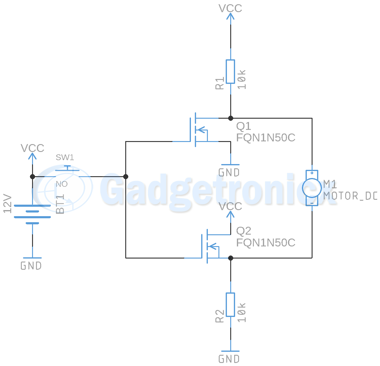
This appears to be a circuit to blow up cmos nand gates, if any of the switches are activated, the output of the gates are shorted.