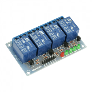
 Sequential device activator or process control timer circuits have wide area of applications and its complexity varies depending upon the device to be activated. Here is a simple sequential device activator circuit using IC 555 and relay as activator. As we all know that IC555 has some unique capabilities to act as a timer and oscillator. Here we employ the IC 555 as a timer to activate three device sequentially given specific timings for each device. The main advantage of this circuit is you can increase the number of devices to be activated just by increasing the count of 555 and you can vary the timings for each device activation. Its very important to understand the operation of IC 555 , so go through this Working of IC 555 before moving to the next section of this Article.
CIRCUIT DIAGRAM:
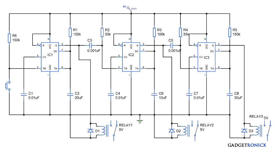 |
| Sequential Device activator using IC555 and Relays |
DESIGN OF CIRCUIT:
Sequential device activator was designed by means of three 555 IC’s which are connected in sequential manner. The connected 555 IC’s above are working in Monostable mode of operation. The monostable mode operation is also known as single-shot since it generates pulse of specified width either high or low. And the above sequential activator was designed by connecting three monostable blocks together.
This forms the basic building block of our activator circuit. In simple the monostable operation of IC 555 can be explained as whenever a positive trigger was given to the pin 2 of the IC, it will give a low output at pin 3. In case of a negative trigger a high signal ( logic 1) will be obtained at the output through pin 3. And the timing of the high pulse depends on the Resistor and Capacitor (RC) connected to the 6 & 7 pin of the IC. The timing can be obtained by using this formula.
T= 1.1 x R x C
By selecting the appropriate RC values using this equation we can achieve required timing for our activation.
WORKING OF SEQUENTIAL PROCESS CONTROL CIRCUIT:
The working of this sequential circuit was achieved by means of connecting the monostable mode circuits in sequence together. That is the output of the first IC will be fed as trigger to the 2nd pin of IC2. So when the 1st block was triggered to give high output, it goes as a positive trigger to pin 2 of the next IC and activate the relay thereby activating the device 1. Since positive trigger was fed to the IC 2 we will obtain no output from it.
When the output of IC1 goes from high to low, it gives a negative trigger to the 2nd pin of the IC2. As a result IC2 will be activated and the resultant high output will obtained at its pin 3. Then the process continues to the IC3 likewise many blocks can be added providing the optimum source to it. Thus the three relays will be activated sequentially with specific timings given by RC components in it.
The timing of the high pulse or period of activation was given by the RC components connected to it. The RC values connected to the blocks are IC1- 150k & 20uF, IC2- 100k & 10uF and IC3- 150k & 30uF. Therefore the timing produced by each blocks will be given by
T1 = 1.1 x 150k x 20uF = 3.3s
T2 = 1.1 x 100k x 10uF = 1.1s
T3 = 1.1 x 150k x 30uF = 4.5s
These are the timing given to the devices in this sequential operation. And by varying the RC values, you can change the timing given by the IC to the relay or device. Then 5v Relay was connected directly to the pin3 of the 555 IC which in turn activate the relay and the device when the IC output was high. A protection diode 1N4004 was added along with it to avoid the spikes produced by the relay when it turned off suddenly. Thus we can achieve sequential device operation using IC 555 with specific timings for each devices.
I have added the Proteus design file of this design below.
NOTE:
When Relays higher than 5V range is used , its preferable to switch ON using transistor drawing supply directly from the source instead of sourcing from the 555 IC.


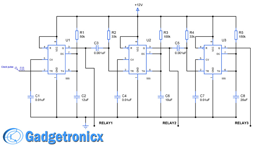
I have to turn on two devices sequentially and turn them of in the reverse order, can I use this circuit?
Can the sequential order of the 555 be repeated ?
Adding more 555’s? Why oh why not just replace all of those 555’s with a simple $1 AVR
yes it was an easy thing to do , but not everyone loves to go for microcontrollers since it requires programming to do so. For those who don’t have programming knowledge, this thing will be an alternative.