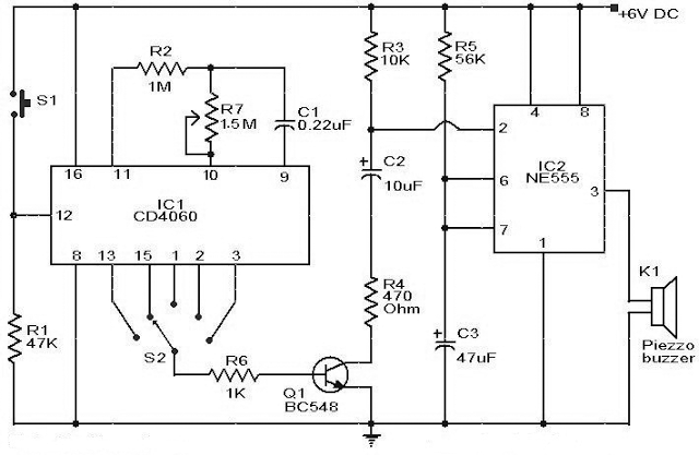
Selective timer alarm circuit using IC 4060 and IC 555 was given above. As we all know that the IC NE555 was a timer and oscillator but the IC1 CD4060 was a 14 stage binary counter with a built in oscillator.The output of the IC1 will become high one after other and one at a time so here we employ that IC as an source for the selective timing to be used.The last five outputs of this IC was used here.Lets move into the working of this circuit.The switch S2 should be a single pole five throw rotary switch.
WORKING OF CIRCUIT:
The IC2 NE555 was wired as a monostable Multivibrator and it was triggered by the high pulses from the IC1 which reaches the 555 via transistor. Since the IC2 was wired as a monostable Multivibrator the buzzer will produce the sound when the trigger pin goes low which happens when IC feed low pulse to transistor base and turn it on. The duration of the buzzer alarm was given by means of two components C3 and R5 connected to IC 555.
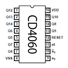 The above given diagram was the pin diagram of the iC CD4060. As i said above the IC CD4060 consists of built in oscillator followed by 14 stage divider. The pulses generated by the oscillator is fed to these divider stages which in turn divides the incoming signal by some factor thus giving different frequency signals from the pins Q4 to Q14.
The frequency of the oscillator depends on the resistor R7 and C1 in the circuit diagram, these components are also referred as RT and CT. The formula governing the frequency of the oscillator is given as
f= 1 / 2.3 x RT x CT
Applying the Resistor and Capacitor values in our circuit we obtain ,
f= 1/ 2.3 x 1.5M x 0,22u = 1.3 Hz.
So this was the basic frequency generated by the in built oscillator of this IC. Now we have used Q9,Q10,Q12,Q13,Q14 in the above circuit. Now obtain the frequency that each of this pins will give as output. So in order to identify the frequency obtained from each pins, we have to divide this frequency by the division factor of each pins. For example lets take pin 13 – Q9 which has a dividing factor of 9 therefor the output will be
29 = 512, so the frequency in this pin will be
f= 1.3 /512 = 0.00253 Hz.
Time period T= 1/f = 395 secs which will be 6.6 minutes of time.
This gives us the time period for which the alarm can be set using this pin Q9. In the same way the time calculations are done for rest of the pins in this IC. You can also use other pins like Q4, Q5 ,Q6,Q7, Q8 and so by using the above calculations.

This circuit not working…… i already try…..
The circuit is not generating any time delays or the time delays is not as expected?
You make it?
Not tested, but logically the circuit should work
for what max time this alarm can be set.???
Reply Soon
Aditya,
I have updated the post with detailed calculation for the time period. Kindly find it and perform the calculation based the pins of your desire.