Model rockets are great things to play with but can be dangerous if handled without care.This Rocket Count Down Launch Controller is very useful when launching model rockets and also offers safety to the user. This launch controller circuit also has of a counter which display counts down from 9 to 0 through a 7 segment display during the launch.
MODEL ROCKET LAUNCH CONTROLLER CIRCUIT:
The controller connects to the igniter through a two-wire cable, (at least 50 feet, the longer the better). The cable attaches to the controller terminals. It connects to the igniter which is inserted into the rocket motor. The ignition cable has two alligator clips at the end of the cable which grab the two igniter leads.
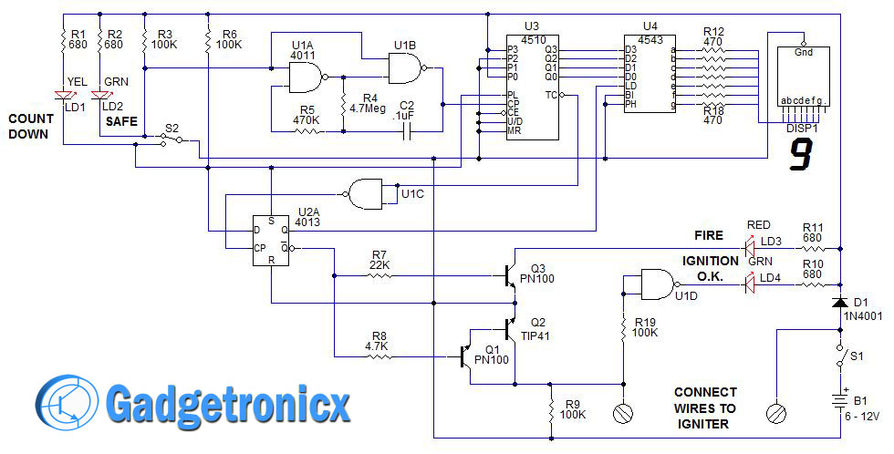
This circuit has a feature that tells you that your igniter is correctly wired and there is continuity through the igniter circuit. If everything is wired correctly, the Ignition OK LED, LD4 (green) lights up when the switch S1(main power) is turned on. There are three LED’s that indicate the status of the controller. LED LD2 (green) indicates when switch S2 is in the “SAFE” position. LD1 (yellow) indicates when push button switch S2 is in the “COUNTDOWN” position(pressed and held down). LD3 (red) illuminates when the countdown reaches 0 and the model rocket is launched.
Referring to the schematic diagram, the circuit blocks will be described. U1A, U1B (CD4011 quad 2-input NAND gate), forms a 1Hz oscillator clock that runs the countdown. When S2 is in the “SAFE” position, U1A, U1B inputs are grounded, which disables the clock. Also, U2A (CD4013, dual-D, flip-flop) is set via R8, causing Q = 1, and Qnot = 0. When Qnot = 0, transistors Q1, Q2 and Q3 are OFF. Q1 and Q2 form a Darlington pair to draw current through the igniter to fire the rocket.
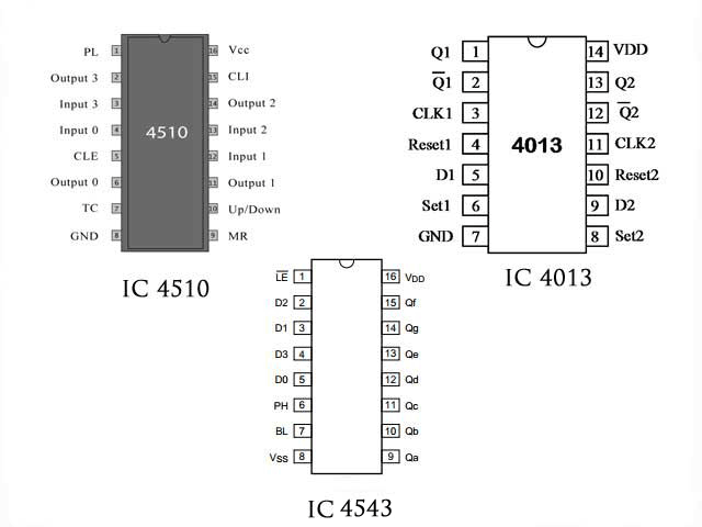
Q3 acts as a display buffer to turn ON the “FIRE” LED when the launch sequence reaches zero. The countdown counter is comprised of two IC’s U3 (CD4510, 4-bit U/D counter with presets) is wired so that when S2 is in the “SAFE” position, P0 – P3 (wired for binary nine), are loaded into the counter when the PL (preset load) pin is high. The CEnot (chip enable low), MR (master reset) and U/D pin are tied to ground which enables the chip, disables the master reset, and makes the counter count down.
The binary output of U3 is connected to Q0 – Q3 of the U4 (CD4543 binary to 7-segment decoder w/phase reverse). U4 takes the binary output of U3 and lights the appropriate segments of the 7-segment display. The common cathode of DSP1 is tied to ground. If you wish to use a common anode, 7-segment display, connect the common anode pin of the display and the PH (phase) pin of U4 to +V. This reverses the output polarity of the CD4543 decoder.
LAUNCH SEQUENCE:
To better understand the operation, let us go through the launch sequence and explain what the circuits do. We have our igniter hooked up via the ignition cable to the terminals of the Launch Controller. The input to U1D is high due to the igniter across the terminals. This causes LD4, Ignition OK LED to turn ON. S2 is in the “SAFE” position so LED, LD2 “SAFE” is ON. U1A, U1B clock is stopped, U3 counter is loaded with 9 and ready to count down. U2A is set (Q = 1, Qnot = 0) enables U4 to update and decode whatever number is presented at the Q0 – Q3 inputs. U2A, Qnot = 0, ensures the firing circuit is OFF.
When S2 is pressed, the inputs of U1A, U1B go high which allows the clock to output pulses once per second. The PL (preset load) pin of U3 is low which allows U3 to count down. U4 decodes U3’s outputs and updates the countdown display DSP1. Pressing S2 also lowers the SET input to U2A which allows for data to be clocked. As a safety feature, the “D” input of U2A is high when S2 is in the “SAFE” position. This prevents any stray noise from possibly clocking an unwanted output condition from U2A. When S2 is in the countdown position, the D (data) pin of U2A is held low.
When U3 reaches 0, the TCnot (borrow/carry) pin of U3 goes low. U1C inverts the signal and presents it to CP (clock pin) of U2A. The D flip-flop switches its outputs, Q = 0, Qnot = 1. When this happens, the Q output freezes the display by taking the LD (load) pin of U4 low. The Qnot = 1, turns ON the Q1, Q2 Darlington pair and powers the igniter to fire the rocket. Q3 turns ON LED LD3 to indicate the firing point was reached.
When S2 is released after the rocket has launched, U2A is reset, the clock is reset, the counter is preset to nine, the “COUNTDOWN” LED is OFF, the “SAFE” LED is ON. The Ignition OK LED should be off indicating an open circuit. S1 should be turned OFF when setting up for your next launch to save your batteries and to assure no possible power is available to the launch controller and igniter. Have fun but be safe. This Model Rocket Launch Controller can help you do that.



Ron,
Was this circuit ever published in a magazine? I’ve been looking for an article with a similar, if not identical, circuit. It was on the cover of the issue, in a black RS project box I think with the metal cover. I thought it was Modern Electronics, but maybe it was Popular Electronics or Radio Electronics? I’ve been searching to no avail.
Thanks!
Brian
Hi Brian, I don’t recall publishing the article in any magazine. The unit was originally designed and built back around 1990’s. The unit is housed in a LMB aluminum enclosure that housed the circuitry and the batteries. I didn’t make Gerber files for this unit when I published it. The circuit is fairly simple and I used point-to-point wiring on a RadioShack 276-147 general purpose prototyping board. If you need further information, let me know
Hi Peter, Another thing to try first is to lower the 4.7K resistor value to 3.3K for 6V, 4.7K for 9V – 12V. If that doesn’t work, use the first solution of adding the extra NPN transistor.
Hey Ron,
I built the circuit, but I used a Darlington pair (TIP120) on the output instead of the PN100 and the TIP41. The problem is I’m only getting 1.3A from at the output, not enough to turn on the igniter. I’m thinking I might need to change the base resistor to the Darlington pair; any suggestions.
Hi Peter, The TIP120 Darlington transistor has internal base emitter resistors that totally change the bias drive requirements. The outputs of the CD4013, actually all CD40XX series CMOS parts have a limited output drive current capability. A PN100 has a gain of 100+ and the TIP41 has a gain of 40. 4000 * 1 mA = 4 A. To use the TIP120, just use the PN100, or 2n4401, or 2N2222, or any general purpose NPN transistor. Connect the base to the 4.7K resistor, the collector to the TIP120 collector, and the emitter to the base of the TIP120. This will provide the additional gain you need to drive the the TIP120 into saturation and provide the output current you need to fire the ignitor. Hope this helps.
Hi Peter, Another thing to try first is to lower the 4.7K resistor value to 3.3K for 6V, 4.7K for 9V – 12V. If that doesn’t work, use the first solution of adding the extra NPN transistor.
Are still available for answering questions. I am wanting to use this circuit for my students in our rocket club? Please reach out to me? Had some questions. Thanks, Dr. G.
Hi Gary, If you have questions, you may ask them here. I would be happy to answer any questions you have.
thats cool gonna try these
Notice Anonymos that the circuit was slightly modified. One resistor was added to protect the input to the U1D quad nand gate. Let me know if you like it when you are done building it.