Interfacing LCD with ARM7 Microcontroller is what we are going to see in this tutorial since LCD’s help us to achieve a cheap Embedded Design with vital information display. This tutorial teaches you about designing and programming of LCD using LPC2124 Microcontroller.
16×2 LCD:
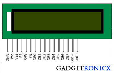 |
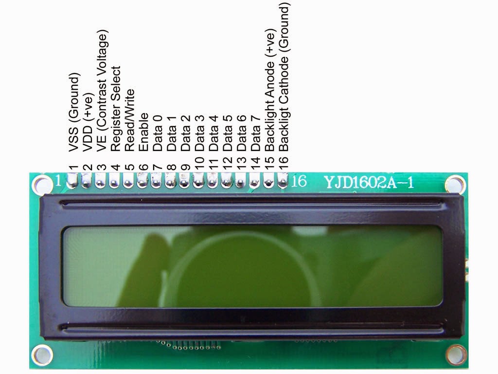
| 16×2 LCD Pin diagram |
This type of LCD is very common consists of 16 columns and two rows. The pin diagram of a 16×2 LCD was shown in the above diagram where DB0 – DB7 forms the data pins, RS – Register select, En- Enable and RW – Read/Write. The detailed pin functions was given in the table below.
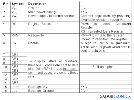 |
| Pin description |
Operation of LCD takes place by means of two inputs one is command and the other one is data. Command makes the LCD to perform actions such as cursor blink, cursor position , LCD on/off etc. Whereas Data will give a specific character to be displayed in the LCD screen.
COMMANDS FOR LCD:
The below table gives the basic commands and its respective operation a LCD will perform.
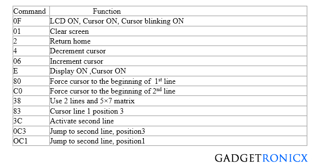 |
| Command table |
DATA/COMMAND TRANSMISSION TO THE LCD:
The data and command transmission to the LCD will flow through the pins DB0-DB7, however the state of the RS pin will decide that the transmitted byte whether a data or command.
- RS = 0 for command transmission.
- RS = 1 for Data Transmission.
- Then pulse the enable pin from high to low that is EN=1 to EN=0 with specific time delay between. Note that pulsing enable have to done for both data and Command transmission.
CODE:
The below code was built using Keil uVision 4 IDE. In the below code a a word “GADGETRONICX” was displayed and then made to scroll continuously using the command “0x18”.
#include<lpc21xx.h>
unsigned char text[12]="GADGETRONICX";
void lcd(char a,int b);
void delay(void);
int main(void)
  {
        int i;
PINSEL0=0;
IODIR0=0x000003ff;          //Set directions
lcd(0x38,0);
lcd(0x0f,0);
for(i=0;i<=11;i++)
lcd(text[i],1);
while(1)
{
lcd(0x18,0);                     //Shift to right
delay();
}
  }
void lcd(char a,int b)
  {
   IOSET0=a<<0;
IOSET0=b<<8;
IOSET0=1<<9;
delay();
IOCLR0=1<<9;
IOCLR0=b<<8;
IOCLR0=a<<0;
  }
void delay(void)
  {
   unsigned int j;
for(j=0;j<=10000;j++);
  }

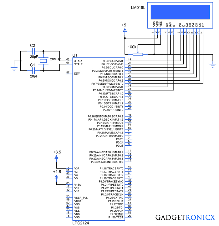
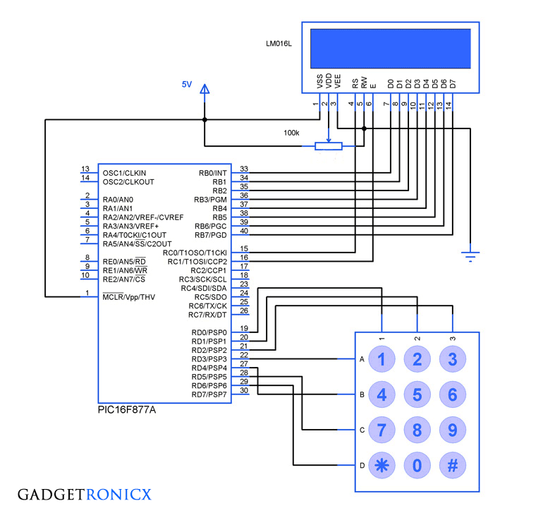
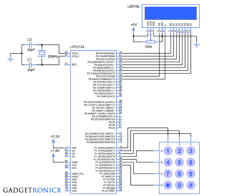
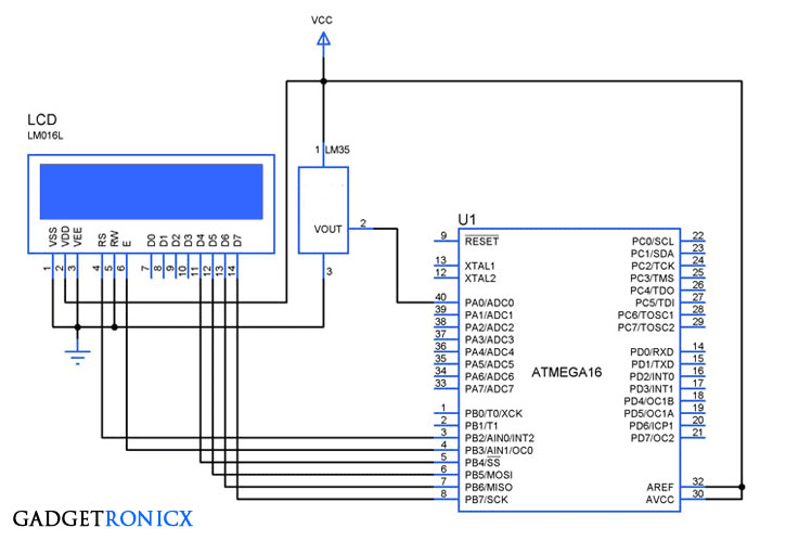
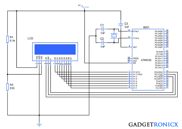
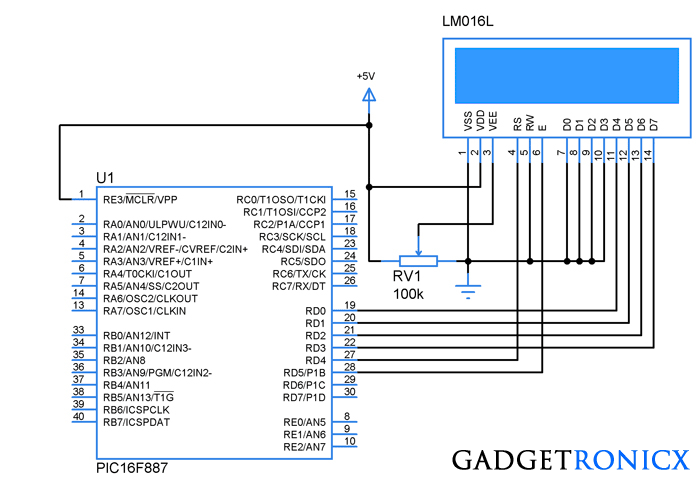
the above circuit u have given is not working in proteus there is no output from port 0 its jus being in disable state i mean a black colour is shown on the pins of port 0
Anil Krishna,
The previous circuit had a simple error with connection of VSS and VDD pin, well it was corrected now. I believe that wrong connections in power pins won’t be an issue in Proteus Simulation. I checked the design and output once again and it works perfectly. So kindly run a check over your design and see if you have connected everything as shown. Or else create a new file and start the design right from the beginning since the software may misbehave and display unexpected results sometimes. Hope this helps, don’t hesitate to ask if you have any other questions.