 |
| Frequency Divider Circuit |
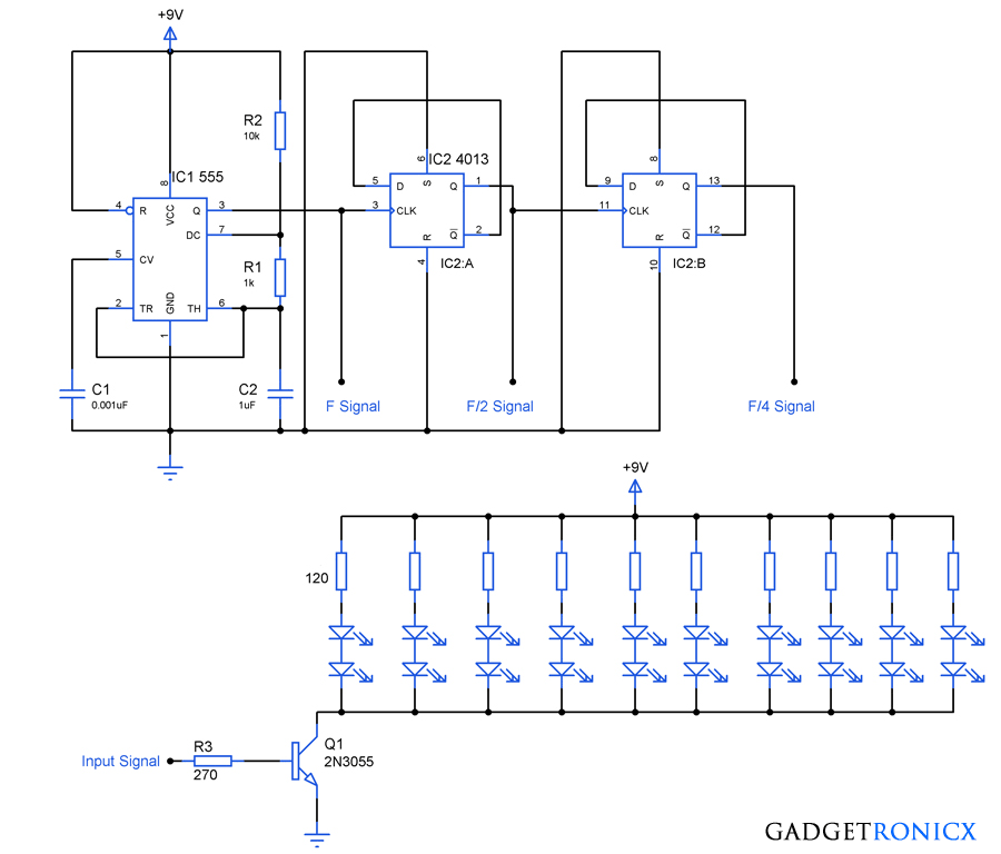
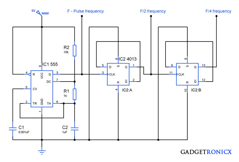
Ever came across a situation where you have only one source of signal with specific frequency and need to obtain signal of several frequencies. If yes, this kind of circuit might be the one you need to use in your design. The above circuit was a frequency divider which is capable of dividing the input clock frequency by means of a certain factor. This Frequency divider circuit was built around Timer IC1 555 which feeds the source pulse and IC2 4013 a dual D type flip flop which divides the incoming pulse frequency.
WORKING OF FREQUENCY DIVIDER CIRCUIT:
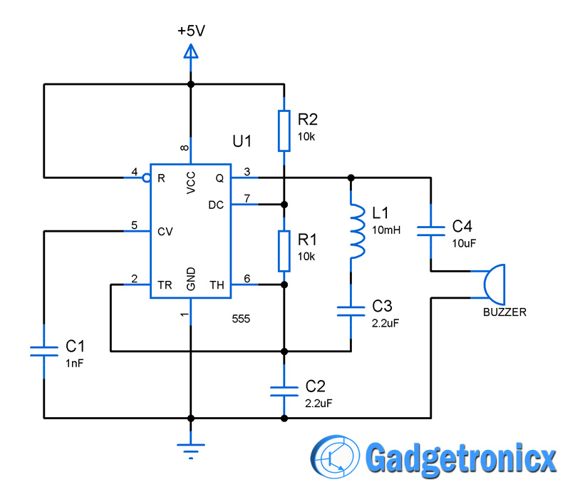
IC 555 was wired as an astable multivibrator and this forms the source of the clock pulse. We have been using this Astable Multivibrator widely so i don’t need to brief up the working explanation. The output frequency produced by the Multivibrator depends on three components R1,R2 and C2. Changing the values of the above mentioned components will result in change of output frequency.
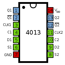 |
| Pin diagram of IC 4013 |
IC 4013 is a dual D type flip flop consists of two flip flops which can be used in a independent manner. In a D Flip Flop D1 & D2 pins are meant for data input which can be either logic 1 or 0. CLK1 and CLK2 are the pins where the clock input for Flip Flop 1 & 2 are fed. This is of edge triggered type so that it switch output states to sudden changes in voltage levels. The S and C are Set and reset pins of the respective Flip Flops.
To wire IC 4013 as a Frequency divider all we have to do is wire the complement pin Q’ to the data input D of the flip flops. The feedback signal of the complement Q pin to the data input divides the clock signal frequency by half. Lets take a look at how the feedback works as a frequency divider.
At the beginning Clock signal and the Q output of the D-type are logic 0. Q’ is the complement output of Q pin so at this case the Q’ pin will be of logic 1. Feedback from Q’ to Data D will make the input pin high. The arrival of first rising edge transfers the logic state at D to the Q pin and this in turn makes the pin goes high. High signal at the Q pin in turn makes the Q’ pin to go low.
The arrival of second edge makes the D low since the current state of Q’ is fed back to it. This makes the Q pin to low state and Q’ to high state. Thus the cycle continues with the following rising edges as the number of output pulses is divided by two compared the number of input pulses and a frequency of F/2 is obtained.
Connecting the next Flip flop in such a way will give a signal of F/4 of the original frequency of the pulse obtained from the Astable Multivibrator. Thus we can obtain F/8, F/16 signals by connecting the Flips Flops in continuous sequence.

