Analog to digital converter circuit are very useful in a digital system where the conversion of raw analog signal to digital data bits possess a notable significance. ADC’s are also quite familiar in several microcontrollers, but using a ADC in micrcontroller requires programming skills and not everyone love to go in to programming. The circuit shown above will offer a solution for those who don’t have any sort of programming skills.
IC ADC0808:
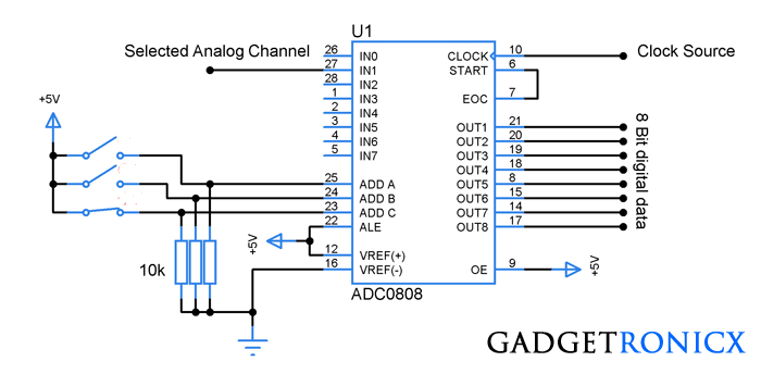
This IC was a simple Analog to Digital converter which provides a resulting 8 bit data for input analog signal. The pins OUT1 to OUT8 gives the output data bits in binary form whereas IN0 to IN7 allows user to feed their analog signal. User can use only one input channel at a time and the channel selection was done by using the pins ADDA to ADDC. The various logic states at these three pins will enable us to select one out of 8 different channels.
The ALE (Address latch enable) pin should be made high to enable the selection of input channels. The EOC(End of conversion) and Start pins are used to control the data conversion. The EOC pin gives high state after conversion and the start of conversion can be initiated by feeding the low pulse to the active low Start pin of the IC. The OE(output Enable pin) was used to enable the digitized output and Clock pin to feed the clock pulse for chip operation.
WORKING OF ANALOG TO DIGITAL CONVERTER CIRCUIT:
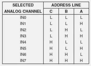
The working of the circuit starts with making ALE and OE pins high which are meant to choose the channel and also enable output. 5 V was the default reference voltage and it can be altered by feeding the voltage of our desire to the pins Vref+ and Vref-. The Channel selection should be done by using the pin ADDA to ADDC pins and here in this circuit diagram input channel 1 was selected. The below table will give the logic states of all pins and their respective channel selection.
Now the Analog signal is fed into the channel you selected and then the state of the pin START should be made low from high to start for activation. And after the conversion the EOC pin goes high and it indicates the conversion is over. The EOC pin retains it low state as soon the next pulse is encountered. As you can see in the above circuit the EOC pin was connected to start pin which triggers a chain reaction resulting in continuous conversion to take place.
Finally we will get a 8 bit data from the pins OUT1 to OUT8 which can be used for further processing and display. You can even connect the LED’s to these pins and visually view the output binary data, Led On indicates binary 1 and off indicates binary 0 data.
NOTE:
- You can control the data conversion by adding a button to the start button which connects to the ground when pressed.
- Adding a indicator LED to EOC pin will help to notify the end of conversion.
- Change the combination of switches as per the logic table to select through the various input channels.
- Since it was a 8 bit ADC the resulting increment in output data will vary per Vref/256 i.e 2^8.


I want 3 volt control, auto start generator circuit and 40 ampere. 240 voltage. autostart changeover switch. first grade electronic and electrical equipment component. I want this is very urgent circuit.
please send me thank you.
How far you have worked on the above project?