Building a RF remote control is not a joke, even with dedicated TX, RX, encoder and decoder chips. I have attempted to build one and struggled quite a lot with it . This is because RF/ Wireless remote control circuits won’t work as expected always. There are number of things that could go wrong with it, I have finally cracked making a DIY remote control which am gonna share with you all.
PROBLEMS WITH HT12E and HT12D RF REMOTE:
To build this I have used HT12E, HT12D and 433Mhz RX and TX. Nothing fancy in it, these are quite common and you might have come across in many RF tutorials and circuits. There are list of problems you might face when building this remote control and I can certainly say that these issues are not straightforward to resolve.
- The decoder chip exhibits active state when powered ON, this will make the outputs active without any user input. This condition is totally undesirable since no one wants their device to get activated by itself without input feed.
- Unstable RF link will fluctuate thus in turn will cause abnormal operation.
- The active low behavior of HT12D will not allow you to drive output activators directly.
- The HT12D chip acts as a latch meaning that the output will not change it’s state unless there is new input fed to it. Imagine if you press a input button and release it, the output from the decoder will be latched and will remain the same even after you turn off the transmitter circuitry.
HT12E:
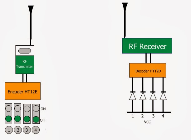
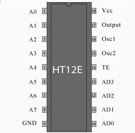
This is an encoder chip that has 4 data and 8 address lines for secured transmission. The input pins are active low, so will get activated only when you feed any low signal. Dout pin is where we will obtain encoded data. This will then go to TX module for transmission. Refer this “Working of HT12E” for more explanation on this chip.
433MHZ TX CHIP:
This is a transmitter chip which uses ASK signalling scheme with the frequency of 433Mhz. This module is quite famous and can be found commonly with online vendors,
HT12D:
This is the matching decoder chip of HT12E. The output pins of this chip exhibits active low as already mentioned, so you cannot directly drive the activators using this chip. VT is a pin which goes high whenever valid transmission is received by the decoder. By the word valid I mean data signal with matching address set by the pins A0 to A8. We will be using this pin to identify whether a signal is received and this will help us in eliminating false trigger. Refer this “Working of HT12D” for more info on this chip.
433MHZ RX MODULE:
This is the matching receiver to the TX which we saw earlier in this article.
RF REMOTE – TRANSMITTER CIRCUIT:
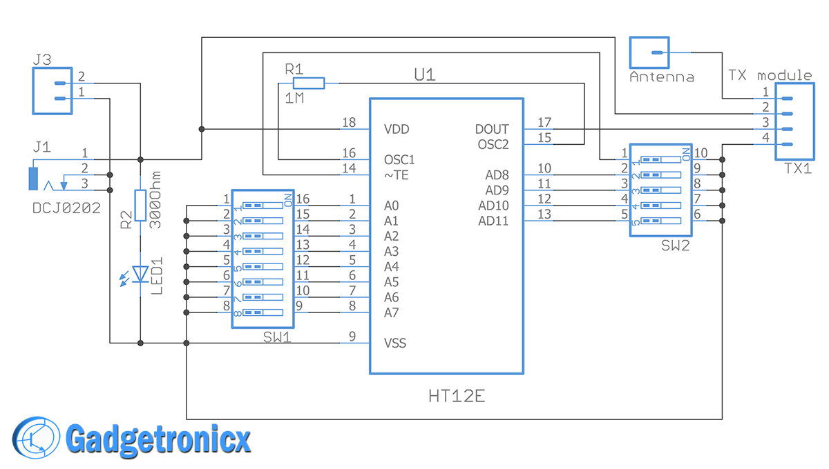 The working of TX circuit is pretty straightforward and easy to understand. The 8 DIP SW1 switch connects the address lines to the ground on activation. This will enable user to set their desired address. Similarly I have added 4 DIP switches SW2 which will connect to ground and feeds data on activation since the data pins are active low. The TE pins controls whether the transmission of data from the chip. LED1 serves as an indicator when the board is ON. The 433Mhz TX module is connected to antenna. This module uses a DC jack or connector J3 for +5V power input.
PCB DESIGN:

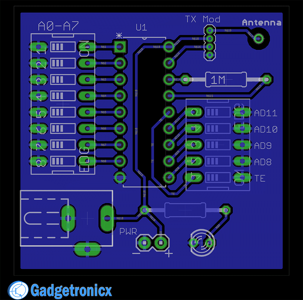
Here is the PCB design of transmitter circuit. Here is the corresponding gerber files to this design which you can use to make your own PCB. You can download the design and PCB files below
BILL OF MATERIALS – RF TRANSMITTER:
| Part | Value | Package |
| ANTENNA | Antenna | 1X01_POGOPIN_HOLE_0.58_DIA |
| J1 | DCJ0202 | DCJ0202 |
| J3 | 1X02 | sparkfun |
| LED1 | LED3MM | led |
| R1 | 1M | 0207/12 |
| R2 | 300Ohm | 0207/12 |
| SW1 | EDG-08 | DIP through hole switch |
| SW2 | EDG-05 | DIP through hole switch |
| TX1 | TX | TX module |
| U1 | HT12E | DIP254P762X342-18 |
RF REMOTE – RECEIVER CIRCUIT:
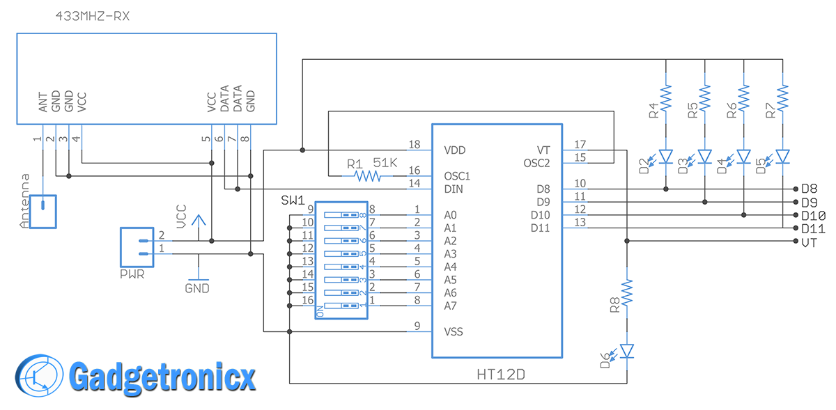
The receiver section of this project is of two sections Decoding (shown above) and Controlling part. In the above decoding section signal from the RX module, HT12D will decode the incoming signal. Use 8 DIP switch to set the address, remember this must be the same as encoder address for making successful reception. D6 lights up as an indication of successful signal reception from transmitter. You will now obtain the output data from the pins D8, D9, D10 and D11. This is a latch output so state of these pins will be remain same unless there is any change in the input signal to HT12E.
CONTROLLING SECTION:
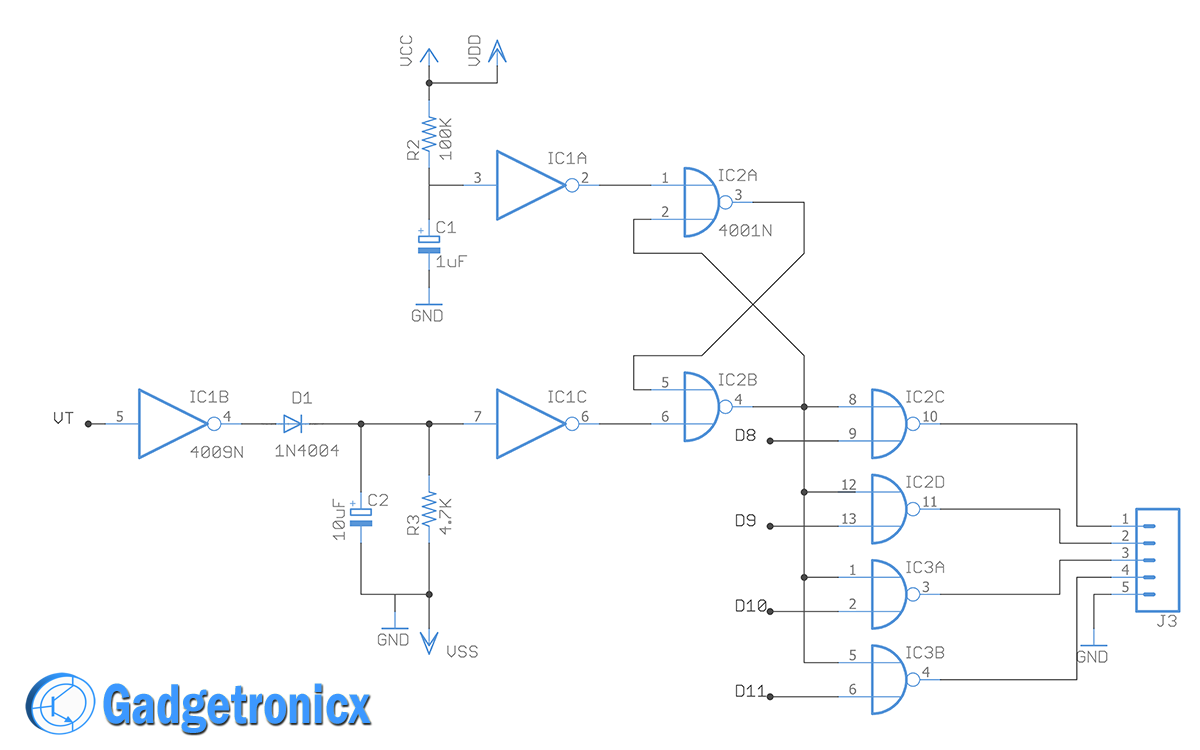
This is where things get tricky in this RF remote making and you might wanna pay close attention to this section. The main purpose of this section is to keep the output data stable , give power on reset pulse to prevent device from starting in undesired state, eliminate the effect of noisy signal and to give momentary remote control experience to the user.
The controlling section is of three separate blocks.
- RC Power on reset – R2C1
- Retriggerable multivibrator – IC1B, D1, C2, R3 and IC1C
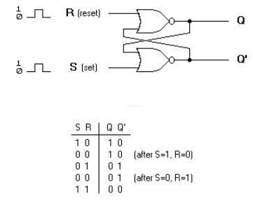
- SR latch – IC2A and IC2B
RC POWER ON RESET:
The HT12D will start up with active state output which is undesirable. I am going to use signal from VT pin to eliminate this issue. This can be achieved with the help of SR latch using NOR gates IC2A, IC2B and NOT gate IC1A. Basically IC2A and IC2B forms a SR latch which is reset through NOT gate IC1A . At power ON C1 will be discharged so IC1A’s input will be low. C1 charges through R1 producing a high level which feeds high input to pin 1 of IC2A which is the reset pin of latch. This will reset the SR latch, from the above truth table we know that output of IC2A will be low and IC2B will be high when the system is ON. This will force low logic in all output pins of IC2C, IC2D,IC3A and IC3D which will be end output of this whole RF unit.
RETRIGGERABLE MULTIVIBRATOR:
VT will give high signal output when there is a valid signal transmission from transmitter. Mostly the signal will be noisy which therefore fluctuates. So to derive a stable signal from VT, a retriggerable monostable multivibrator stage using IC1B, IC1C, D1, R3 and C2. Unstable VT signal will act as a trigger pulse, when VT is low output in IC1B goes high, which will charge the capacitor C2. When the capacitor is fully charged, the input to IC1C becomes high which in turn gives low as output. Similarly when VT goes high, the output of IC1B will be low which will discharge the capacitor through resistor R3 and once it’s done output of IC1C will switch to high state. The real magic lies with C2R3 pair which acts as a timing element in this circuit. And finally we will get stable VT signal as output.
SR LATCH:
The output from retriggerable mutlivibrator goes into Set pin of SR latch. Upon receiving valid data by the receiver, Set pin (pin 6 of IC2B) of SR latch will go high and this will result in low state output of IC2B. Remember Reset pin of SR latch that is 1st pin of IC2A would have been in logic 0 because of our Power on Reset pulse arrangement. Now that we have resolved the unstable VT signal, Power On reset and anonymous triggering of output all we have left is obtain the data in high logic so that it can drive components or activators.
The output from IC2B is used along with the actual Data output from the pins D8,D9, D10 and D11. Individual NOR gates like IC2C were used to combine the output of IC2B and D8. When AD8 is activated at the Encoder input, receiver will receive this signal decode them and exhibit it at D8 pin of the decoder which is active low. Upon successful reception output of IC2B will go low as explained above and combined with D8 which is active low using NOR gate IC2C. This in turn will give high output at output of IC2C which is the final output of D8 and can be used drive components or activators directly.
Similar things occur when AD8 is not activated at the encoder, D8 will be high therefore output of IC2C will be low. The same working principle applies for other data output pins. And your RF remote if finally ready to use.
PCB DESIGN OF RF RECEIVER:
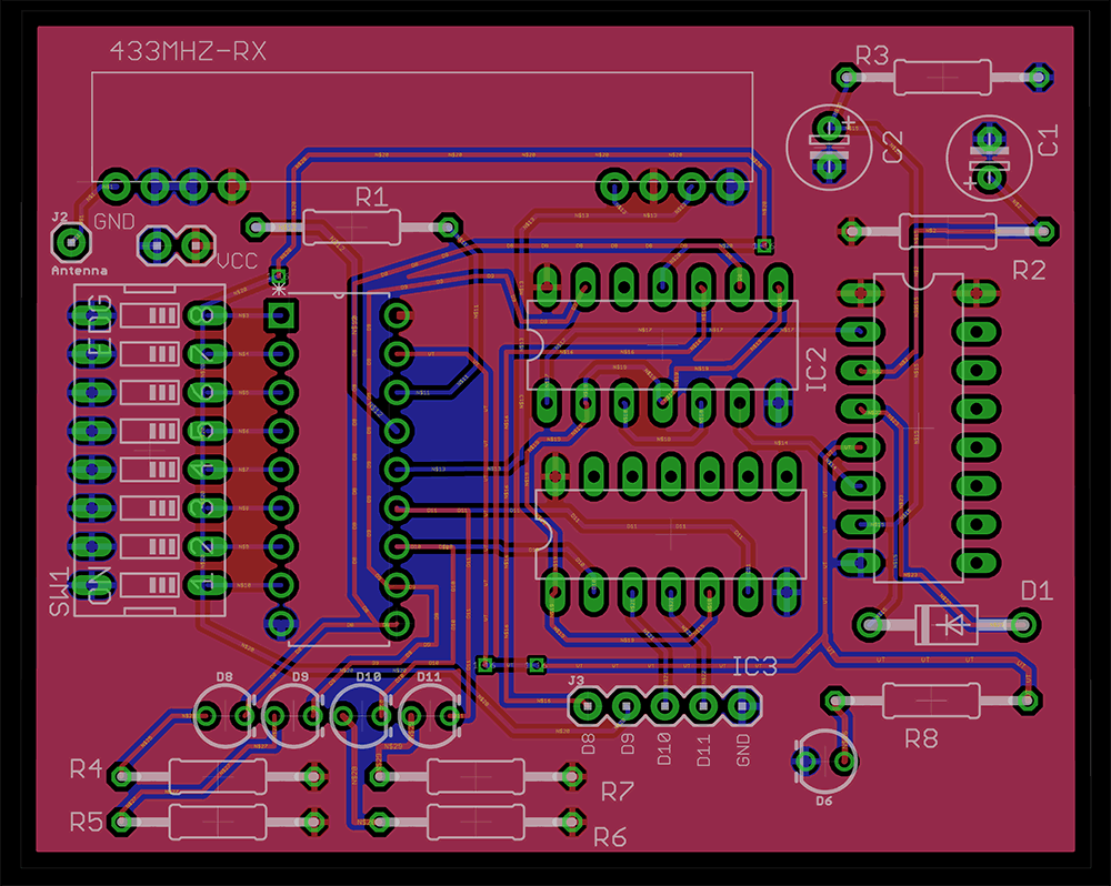
This is the PCB design of the whole receiver circuit including the controlling unit. Connector J3 is where you could see the output pins and a Ground pin. This is to use this board with actuators and other microcontrollers. You can download all the schematic, design and gerber files for the receiver from below.
BILL OF MATERIALS – RF RECEIVER:
| Part | Value | Package |
| 433MHZ-RX | 433MHZ-RX | RF module |
| C1 | 1uF | E2 |
| C2 | 10uF | E2 |
| D1 | 1N4004 | DO41-10 |
| D6 | LED_3MM-NS | SparkFun-LED |
| D8 | LED_3MM-NS | SparkFun-LED |
| D9 | LED_3MM-NS | SparkFun-LED |
| D10 | LED_3MM-NS | SparkFun-LED |
| D11 | LED_3MM-NS | SparkFun-LED |
| IC1 | 4009N | DIL16 |
| IC2 | 4001N | DIL14 |
| IC3 | 4001N | DIL14 |
| J1 | PWR | 1X02 |
| J2 | Antenna | 1X01 |
| J3 | 1X05 | sparkfun |
| R1 | 51K | 0207/12 |
| R2 | 100K | 0207/12 |
| R3 | 4.7K | 0207/12 |
| R4 | 0207/12 | rcl |
| R5 | 0207/12 | rcl |
| R6 | 0207/12 | rcl |
| R7 | 0207/12 | rcl |
| R8 | 0207/12 | rcl |
| SW1 | 8 pin DIP switch | SW-DIP-8 |
| U1 | HT12D | DIP254P762X342-18 |
TESTING AND DEMONSTRATION OF RF REMOTE:
Hope this article and video be of great use in building your RF remote. Please do post your outcomes and share your feedback with me. Happy DIY 🙂





Hello Frank, I have a question, this RF transmitter-receiver works well as it is presented by you, yes or not? Thanks,
Regards,
Cesar
Hello Frank, I like your project, but I don’t know what is J3 component? what are the values for the resistors (R4 to R8) in RF receiver, it says 020712 RCL, thanks for your help.
Regards,
Cesar
HI Frank.
Congratulations on a credit worthy circuit. However there are a few ways that the circuit can be improved. Gates IC1B and C you call a monostable is not necessary. By the way for a circuit to be a monostable it must have some sort of feedback. This is what keeps it in one (MONO) stable state. It is also not good design to directly drive a capacitor from the output of a gate. Even via a diode. Capacitor in-rush current is in theory unlimited, at least for a very short time. This current must come from the gate. Not a good idea.
The reason your VT line is not stable is the fault of the Receiver. Either you are at the extreme limit of radio range or there is a mismatch between the encoder/decoder. This is usually cased by the oscillator components not matched correctly.
If you connect your controlling input of your 4 output gates to the VT line the rest of your circuit is not needed. You also have a problem with the Flip Flop. At power on the FF will be reset then set when the first command comes in from the decoder but after that the FF needs to be reset again at power on.
You may like to look at using a small cheap micro controller chip. It can replace all of your circuit after the decoder chip. Hope this helps.
Cheers – Jeff
Thank you very much Jeff for giving a detailed feedback on this circuit. I did considered a MCU but then I thought to do it using some bunch of chips. Now am considering to make a version 2 of this project with the improvements suggested. Thanks again 🙂
Can I have full schematic diagram of decoder with all logic ic
It’s given in the article. The circuit is split into two parts for better understanding. Check these links for the circuit diagram in full resolution https://www.gadgetronicx.com/wp-content/uploads/2017/08/RF-rx-control.png
https://www.gadgetronicx.com/wp-content/uploads/2017/08/RX-circuit.png
I ordered the Gerber files pcb from jlCpcb,but the receiver has 3 ic can you tell me or least send what the 14 pin ic3 is and the labels of all the components on transmitter and receiver
Hi Kevin,
Updated the article with respective BOMs for both transmitter and receiver section. Hope it helps and let me know how it turns out 🙂
How to adjust length of antenna.
I got thai ic 1 is ht12d in decoder but what is ic 2,3,4 ..?
Check the controlling section circuits, you will get better idea about this project.
I used ht12e &ht12d ,Igot no signal,so I tried pt2262&pt2272,also no result,please try help me,.
Hi, I already made the remote and receiver circuit and I wanted to ask for some help if you would be so kind, I don’t really understand the schematic, I don’t know exactly what parts do I need and what values, I have no idea what IC’s you are using, I am talking about the circuit that solves the problems on the receiver side(ic1b, ic2d,etc), could you give me a list of the parts, what type of transistors, ic’s etc, and a layout schematic which is easier for me to read? Thank you so much for your help.
Hi Alex,
Yes this circuit can be hard to understand. But as far as I see the circuit diagram is clear with all parts marked with part name and numbers. And I have written this article as descriptive I can since this might be bit hard to follow. Go through the article again and work out the logic in a piece of paper, it might help.
Why I can’t download the transmitter circuit?
Sorry about that. The file can be downloaded now