Amplifiers are very necessary element in any project dealing with signal strength and quality. Similarly Audio amplifiers are used to amplify the strength of speech signals and makes it more audible by amplifying it and put it through a speaker. Here we are going to see construction and working of a 2 stage amplifier circuit using Transistors.
WORKING EXPLANATION:
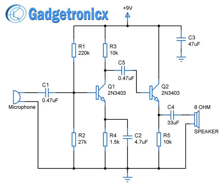
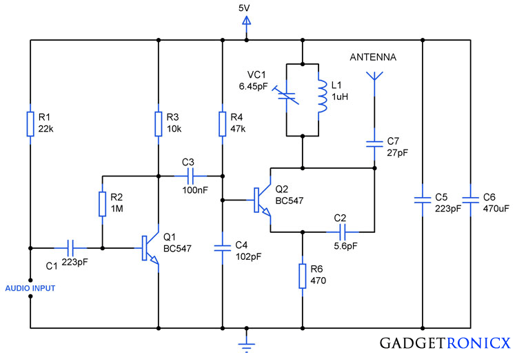
This 2 stage amplifier circuit comprises of two stages each of which perform amplification on the incoming audio signals and output finally obtained at the end of 2nd stage. A simple Microphone was used to feed input audio signals followed by a coupling capacitor C1 which removes any DC element from audio signal.
FIRST STAGE:
In the first stage the transistor was wired in Collector emitter amplifier. R1 and R2 forms a voltage divider in order to provide the bias voltage for the transistor to turn it ON. R3 serves as the Load resistor for the transistor to amplify the voltage of the input signals. The variation in base current of transistor from the Microphone controls the Q1 and voltage developed in R3 will be inverted with respect to the input signal from the Microphone.
Thus amplified signal is obtained from R3 and goes to the next transistor stage through a coupling capacitor C5 to remove the DC element from the signal. R4 serves the purpose of providing feedback to stabilize the DC bias given to the Q1 transistor. C2 was used to maintain the gain at which the voltage of the input signal in amplified by this stage.
SECOND STAGE:
This stage was used to amplify the current of the audio signal and configured as an emitter follower stage. The load resistor is omitted here to decrease the output impedance and amplify the current of the signal. The Resistor R5 goes in to same swing equivalent to the signal from output of first stage.
Thus Voltage and Current amplified signal can be obtained from the Emitter terminal of the Transistor Q2. This improves the overall power of the signal making it suitable to drive the output speaker connected to it. The signal is then passed through a capacitor C4 which blocks the DC element from the output signal. C3 a decoupling capacitor was used to keep away the stray noise and avoid oscillations affecting the circuit.
Thus the final output signal will be both current and voltage amplified and can drive the Speaker directly and capable of producing loud and clear sound from it.


You’ve left the second stage without bias. The result will be massive distortion or no sound at all, depending on level of input.
Can I have the transistor component as a multisim component
How much is the cost for constructing two stage amplifier
It seems Q2 is not biased.
It is required to provide a Q2 biasing, which could be done by means of a 100k resistor from 9V power supply to the Q2 base terminal. Of course, a proper design depends on the load impedance.
please solve for the output resistance of the emitter-follower stage.
Can you help me to solve this circuit diagram?